

With high NA EUV, Intel foundry opens new frontier in chipmaking
The new tool has the ability to dramatically improve resolution and feature scaling for next-generation processors by changing the optics design for projecting printed images onto a silicon wafer.
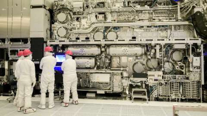
Intel Foundry reported a key milestone in advanced semiconductor manufacturing with completed assembly of the industry’s first commercial High Numerical Aperture (High NA) Extreme Ultraviolet (EUV) lithography scanner, located at the company’s Hillsboro, Oregon, R&D site. Intel’s TWINSCAN EXE:5000 High NA EUV tool from lithography leader ASML is now going through calibration steps in preparation for production of Intel’s future process roadmap. The new tool has the ability to dramatically improve resolution and feature scaling for next-generation processors by changing the optics design for projecting printed images onto a silicon wafer.
“With the addition of High NA EUV, Intel will have the most well-rounded lithography toolbox in the industry, enabling the company to drive future process capabilities beyond Intel 18A into the second half of this decade.”, Mark Phillips, Intel Fellow and director of Lithography, Hardware and Solutions for Intel Foundry Logic Technology Development
Why It Matters: High NA EUV tools will play a critical role in advanced chip development and the production of next-generation processors. Intel Foundry — the industry’s first mover on High NA EUV — will be able to deliver never-before-seen precision and scalability in chip manufacturing, enabling the company to develop chips with the most innovative features and capabilities that are essential for driving advancements in AI and other emerging technologies.
ASML recently announced it has printed the first-ever 10 nanometer (nm) dense lines in the High NA lab at the company’s headquarters in Veldhoven, Netherlands. These are the finest lines ever printed, setting a world-record resolution for an EUV lithography scanner. This demonstration validates the innovative High NA EUV optics design from ASML partner Zeiss.
Groundbreaking images were printed after the tool’s optics, sensors and stages completed coarse calibration — a stepping-stone to running at full specification. ASML’s ability to print 10nm dense lines with a full field optical lithography system is a key step toward readying the High NA EUV tool for commercial use.
How It Works: When combined with Intel Foundry’s other leading process technology capabilities, High NA EUV is expected to be able to print features up to 1.7x smaller than existing EUV tools. This will enable 2D feature scaling, resulting in up to 2.9x more density. Intel continues to lead the way forward for ever-smaller, ever-denser patterning that drives Moore’s Law across the semiconductor industry.
Compared to 0.33NA EUV, High NA EUV (or 0.55NA EUV) can deliver higher imaging contrast for similar features, which enables less light per exposure, thereby reducing the time required to print each layer and increasing wafer output.
Intel expects to use both 0.33NA EUV and 0.55NA EUV alongside other lithography processes in developing and manufacturing advanced chips, starting with product proof points on Intel 18A in 2025 and continuing into production of Intel 14A. Intel’s approach will optimize advanced process technology for cost and performance.